Did you know that the global market size of PCB Design Software market is expected to reach $805.7 million by 2031, at a CAGR of 5.5% between 2024-2031?
It sheds light on the pivotal role of PCB design in shaping the future of electronic devices. It is impossible to overestimate the importance of printed circuit board (PCB) design in a world where technology drives progress.
As you navigate this innovation landscape, choosing PCB design software is critical for engineers, entrepreneurs, and enthusiasts. Understanding the PCB design and the criteria for selecting the most suitable software for your needs is essential.
Let us go through the criteria for choosing the right software to explore recommended options. Whether you’re an engineer or a budding entrepreneur, selecting the right PCB design software is crucial for transforming your ideas into tangible electronic devices.
The PCB Design Landscape
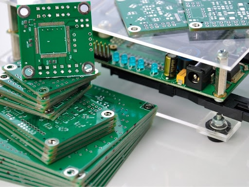
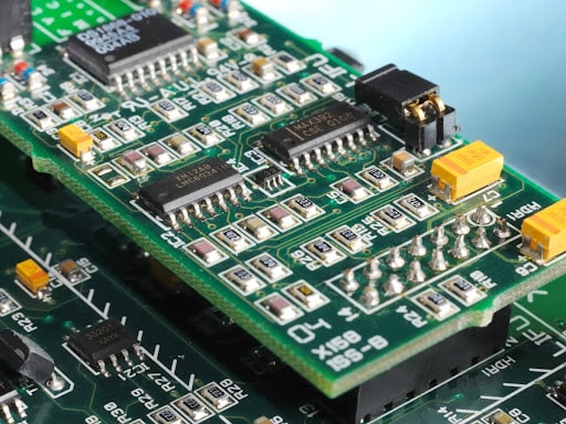
Before choosing any particular software, understanding the wide range of PCB design options is critical. PCBs connect different parts of an electronic device and allow for smooth operations, acting as the nervous system of the gadget. PCBs are used in many modern technological applications, ranging from consumer electronics to aircraft.
The role of a PCB design software is becoming essential in ensuring electronic device performance and dependability that meets the highest manufacturing standards.
Who Needs PCB Design Software?
The software serves many users, including manufacturers, electronics experts, and business owners. It is essential for creating electronic devices to convert abstract designs into physical circuit boards while maximising usefulness, connectivity, and layout.
Engineers: Whether designing complex systems or prototyping new inventions, PCB design software is indispensable if you seek precision and efficiency.
Entrepreneurs: Without having to make significant expenditure for outsourced design services, the software enables startups and small enterprises looking to enter the hardware development space to make their ideas a reality.
Design Creation Enthusiasts: It is a platform for learning and creativity, encouraging invention at all skill levels, from instructional projects to do-it-yourself enthusiasts.
Criteria for PCB Design Software
When selecting PCB design software, several criteria should guide your decision-making process:
Highly Intuitive
As efficiency is key in PCB design, it offers a user-friendly interface with intuitive tools and functionalities, enabling beginners and experts to navigate the design process effortlessly. From schematic capture to layout and routing, a well-designed user interface streamlines workflows minimizes learning curves, and maximizes productivity.
Intuitive features such as drag-and-drop functionality, context-sensitive menus, and real-time feedback enhance usability, allowing designers to focus on creativity rather than technical hurdles. Whether designing your first PCB or refining a complex project, the software should empower you to actualise your ideas to fruition efficiently.
Reasonably Priced
The software should provide value for money without sacrificing quality by striking a balance between features and price. Although some premium solutions include advanced functions, individuals on a constrained budget might be unable to afford these due to their high costs.
On the other hand, downloading a slightly lesser priced or free software can have unintended consequences like insufficient features, inadequate support, or compatibility problems. By selecting moderately priced software, you can leverage robust capabilities without going over budget, guaranteeing a long-lasting investment that evolves with your changing requirements.
Standard and Widespread Use
Choosing software with a large user base guarantees access to a thriving community for support, resources, and collaboration. Compatibility with industry standards enhances interoperability and facilitates seamless integration into existing workflows.
When selecting PCB design software, consider its adoption within your target industry and among peers. A software ecosystem with a large user base fosters knowledge sharing, innovation, and peer-to-peer support networks, enriching your design experience, and accelerating project timelines.
Furthermore, extensive adoption frequently indicates continued development, updates, and support, ensuring long-term sustainability & compatibility with changing technology.
Large Libraries of Components
A broad library of components is required for rapid prototyping and design iteration. The software should include a comprehensive library of symbols, footprints, and models for various electronic components, reducing time & effort when obtaining or designing unique components.
From resistors and capacitors to microcontrollers and connectors, an extensive collection of pre-built components speeds up the design process, reduces errors, and encourages reuse across projects. By leveraging a vast library of components, designers can focus on innovation and differentiation rather than mundane component creation or verification tasks.
Recommended Software Options
Now, let’s explore some of the top PCB design software options that meet the criteria above:
-
Altium Designer
Altium Designer solves all your PCB layout design project needs, from basic circuits to complete avionics systems. Altium Designer stands out as a versatile and feature-rich PCB design tool that is trusted by experts all over the world.
Altium Designer’s unified design environment, robust routing features, and broad component libraries enable users to bring their unique ideas to life quickly.
Altium Designer supports users worldwide, from automotive and aerospace to consumer electronics and medical devices. It has everything in one place, and a unified design environment makes this one of the most preferred PCB design software.
-
Cadence Allegro
Cadence Allegro brings a bleeding edge and your innovations to reality. Cadence Allegro provides various PCB design & analysis tools that cater to novices and seasoned experts.
Its extensive feature set, which includes constraint-free design & real-time collaboration, makes it the top choice for complicated PCB projects across industries.
Cadence Allegro PCB Designer is a scalable and well-proven PCB design environment that addresses methodological & technological issues while stabilizing design cycles.
-
KiCad EDA
KiCad EDA is an open-source PCB design software that has become popular due to its community-driven development model, scalability, and flexibility.
KiCad EDA is an excellent tool for small enterprises because it offers many functions without requiring licensing, such as schematic capture, PCB layout design, and 3D visualization.
KiCad EDA is easy for beginner PCB designers and robust enough for intricate contemporary designs. With an advanced interactive router and improved visualization and selection tools, PCB layout design tasks are now more manageable.
-
OrCAD Capture
OrCAD Capture, a component of the OrCAD PCB design package, provides a complete schematic design and simulation solution. OrCAD Capture simplifies the design process from concept to production because of its user-friendly interface, powerful simulation capabilities, and seamless connection with industry-standard tools.
OrCAD Capture simplifies creating and managing schematic designs by providing quick and intuitive schematic entry, rule definition, instant design feedback, and direct connection with simulation and PCB layout design.
-
Allegro PCB Designer
Allegro PCB Designer, another Cadence product, combines ease of use with powerful capability to provide great PCB design experiences. Allegro PCB Designer enables users to confidently tackle complicated design challenges, including high-speed routing and signal integrity analysis.
Cadence Allegro PCB Designer converts basic and complicated design concepts into reality via a constraint-free design system, ensuring functionality & manufacturability. Scalable technology enables designers to meet all current and future technological and methodological requirements cost-effectively for teams, organizations, and all sizes of projects & intricacies.
Conclusion
PCB design software can improve the PCB layout design in various ways, including component alignment, rule checking, and trace routing. If you want to become more efficient, improve your design, increase precision, or save money, then use PCB design software for your circuit board projects.
Whether you prioritize ease of use, price, or advanced functionality, there is a solution for you. You may confidently utilize PCB design software by considering key aspects like intuitiveness, affordability, industry adoption, and component libraries.
So, begin on your innovation adventure and choose the technology that is ideal for you.