In the ever-evolving world of electronics, precision, and dimensional control are paramount to the success of Printed Circuit Board (PCB) manufacturing. You can’t imagine a world without the ubiquitous printed circuit board (PCB).
Almost all electronic gadgets, including computers, cell phones, medical equipment, and industrial gear, are built around these fundamental parts. The quest for miniaturization and enhanced performance in electronic devices has pushed the boundaries of PCB manufacturing. Achieving excellence in this domain hinges on mastering dimensional control and precision requirements.
However, this guide will explore how PCB board manufacturer meet these challenges head-on, ensuring the production of high-quality, reliable, and efficient printed circuit boards.
The Microscopic World of PCBs
Before we move forward, it becomes essential to understand the microscopic world of PCBs.
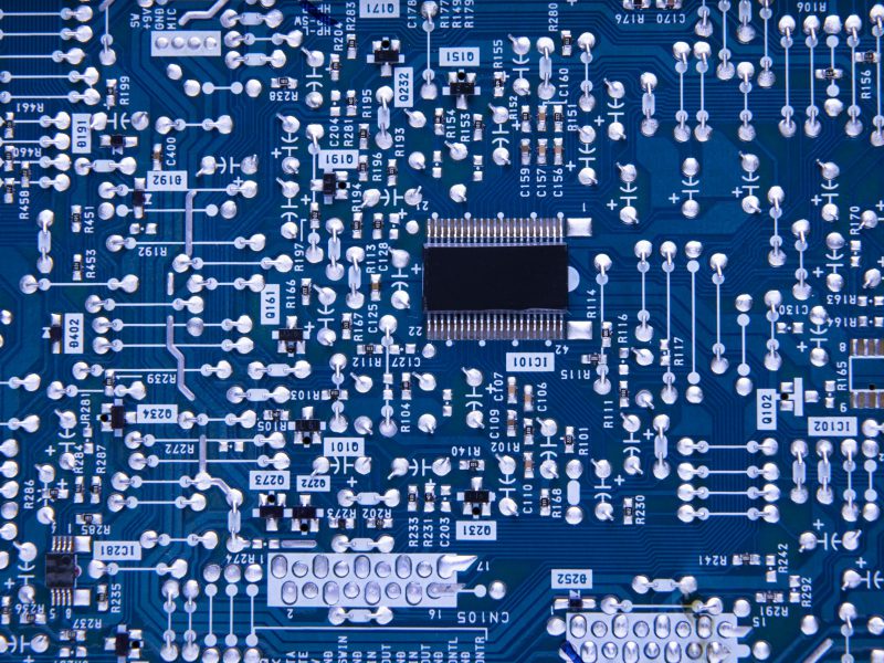
Imagine a miniature city with roadways (conductive traces) connecting the buildings (electronic components). This example captures the world of PCBs aptly. However, unlike a city with wide pathways, PCB has miniaturization of components, extremely thin traces, and crucial spacing between them. This relentless miniaturization pushes the boundaries of PCBA manufacturing capabilities, demanding ever-tighter control over dimensions.
The Importance of Dimensional Control
Dimensional control refers to the ability of a PCB manufacturer (PCBM) to replicate the design specifications on the final product precisely. This encompasses various critical aspects that ensure the reliability and performance of the PCB:
- Hole Size and Location
Drilled holes are necessary to install components and create vias (plated holes linking layers).
Variations in their dimensions or arrangement may result in misaligned components, electrical shorts, or open circuits, jeopardizing the board’s overall performance.
- Trace Width and Spacing
The width and spacing of the conductive traces determine their signal integrity and current-carrying capacity. Inaccuracies can impair the device’s performance by causing overheating, signal deterioration, or total circuit failure.
- Layer Registration
Multiple layers of conductive designs are stacked on multilayer PCBs. Their alignment must be precise for adequate electrical connections between these layers. Misalignment may result in decreased device dependability and connectivity problems.
- Surface Finish
The copper pads’ surface finish is essential for components to solder and be reliable over the long term. A high-quality finish ensures strong solder joints and prevents issues such as oxidation and corrosion.
Precision Requirement: A Balancing Act
The precision required in printed circuit board manufacturing varies depending on the application. High-frequency circuits for communication devices demand tighter tolerances compared to simpler consumer electronics.
However, tighter tolerances come at a cost. Manufacturing processes become more complex and expensive. PCB manufacturers (PCBMs) must balance achieving the necessary level of precision and maintaining cost-effectiveness.
Here’s a breakdown of some industry-standard tolerances for different PCB features:
- Hole size: ≤4.00mm +/- 0.10mm (for standard) and ≤4.00mm +/- 0.05mm (for minimum)
- Trace width: ±0.1 mm (for wider traces) to ±0.025 mm (for fine-line circuits)
- Trace spacing: ±0.1 mm (for wider spacing) to ±0 .05 mm (for high-density boards)
- Layer registration: ±0.05 mm (typical)


How to Achieve Precision?
Achieving precision in PCB manufacturing is a multifaceted endeavor that requires the integration of advanced technologies and meticulous process control.
Different PCB manufacturers use different welding processes and techniques to ensure dimensional accuracy and reliability in their products.
Here are some key methods used in the pursuit of precision:
- Advanced Drilling Technologies
Advanced technologies like laser drilling provide excellent precision when drilling holes with tight tolerances. The high precision of laser drills reduces the possibility of misalignment and variations in hole sizes, which are crucial for the functionality of multilayer PCBs.
Laser drilling also makes it possible to accurately form vias and mounting holes, which ensures dependable electrical connections and component placement.
- Photolithography
Photolithography is a light-based process that plays a pivotal role in PCB manufacturing. This technique involves transferring intricate designs onto the copper foil using a photosensitive film.
By exposing the film to ultraviolet light through a photomask, printed circuit boards manufacturers can create highly detailed patterns that define the PCB’s conductive traces.
The precision of photolithography ensures that the traces meet the required width and spacing specifications, which is crucial for maintaining signal integrity and current-carrying capacity.
- Advanced Etching Techniques
Advanced etching processes guarantee that the traces have the proper width and spacing and allow precise control over the PCB manufacturing process.
This allows for the retention of the desirable circuit layouts on the PCB after the etching process removes the unwanted copper.
Accurate etching is essential to prevent problems like openings and shorts, which can seriously impair the PCB’s functionality. Chemical and plasma etching are commonly used techniques with excellent consistency and precision.
- High-resolution Imaging
High-resolution imaging technologies, including optical and X-ray inspection systems, are essential for verifying feature sizes and layer registration with high accuracy.
Optical inspection systems use cameras to detect surface defects and measure trace dimensions, while X-ray systems provide detailed views of internal layers and vias.
These imaging techniques enable PCBMs to identify and rectify any discrepancies early in production, ensuring that the final product meets stringent quality standards.
- Statistical Process Control
Statistical Process Control (SPC) is a critical method used by printed circuit board manufacturers to monitor and adjust their manufacturing processes.
PCB board manufacturers can continuously collect and analyze data to identify trends and variations that may lead to dimensional inaccuracies.
SPC allows for real-time adjustments to maintain consistent quality and minimize deviations. This proactive approach ensures that the manufacturing process remains within the desired tolerances, contributing to the overall precision of the PCB.
The Benefits of Precise PCBs
If you think of investing in precise PCB Manufacturing, then that can help you yield several benefits-
- Improved Electrical Performance
Precise dimensions enable excellent signal integrity and minimize electrical noise.
- Enhanced Reliability
Accurate feature PCBs are less likely to fail due to misaligned components, openings, or shorts.
- Reduced Rework and Scrap
Accurate production lowers the requirement for rework and the need to discard bad boards, which saves money.
- Miniaturization Potential
Precise control allows for further miniaturization of electronic components and PCBs, enabling the development of more compact and powerful devices.
Conclusion
Dimensional control and precision requirements are paramount in the competitive world of PCB manufacturing. PCBMs who excel in this area can deliver high-performing, reliable boards that meet the electronics industry’s ever-increasing demands.
As technology continues miniaturizing, pursuing ever-tighter tolerances will remain a driving force in printed circuit board manufacturing excellence.