Customized electrical product design is essential in today’s rapidly changing technological environment to fulfil the specific requirements of both businesses and consumers. The market for custom electronics is expanding quickly, encompassing anything from wearable technology to specialized industrial machinery.
This article gives a thorough overview for enthusiasts and professionals, delving into the complex process and stages of building bespoke electronic components.
Understanding Customized Product Design
“Customized electronic product design” involves creating electronic systems or gadgets tailored to meet specific needs and requirements. Unlike off-the-shelf items, these designs are unique and customized to deliver enhanced performance, functionality, and user experience.
According to a report by Fortune Business Sights, the custom electronics market is expected to reach USD 1467.94 billion by 2032, growing at a CAGR of 7.63 percent.
This growth reflects the increasing importance and adoption of customized electronic product design across various industries, driven by the need for more specialized and innovative solutions.
Benefits of Customized Electronic Product Design
While designing a customized electronic product, you may face some benefits, which are mentioned below-
- Tailored Solutions: Custom designs are created to meet the unique needs of a business or consumer, ensuring that the product performs precisely as required. When you focus on specific functionalities, customized products will offer superior performance compared to generic alternatives.
- Competitive Advantages: Innovative features and the latest technologies can be incorporated into custom designs to give them a competitive advantage. Unique products can help a brand stand out, fostering stronger brand loyalty and recognition.
- Efficiency and Optimization: Custom products can be developed to use resources efficiently, cutting waste and increasing productivity. While customized items may have a greater initial cost, they might save money over time by increasing efficiency and lowering the need for adjustments.
- Flexibility: Custom items are more accessible to upgrade or modify to meet evolving needs or take advantage of new technology. Designs can easily accommodate future expansions by scaling with the business’s growth.
- Improved User Experience: Custom products can provide a better user experience by concentrating on the unique needs of the end-user. Products that meet user needs precisely can lead to higher satisfaction and reduced support costs.

The Importance of Customized Electronic Product Design
Customized electrical product design is essential because it provides solutions that standard designs cannot. This strategy promotes efficiency, creativity, and the creation of cutting-edge technologies tailored to specific markets.
According to a Grand View Research report, the global electronics manufacturing services market was valued at USD 515.1 billion in 2022, reflecting the ever-growing need for custom-designed solutions. Between 2023 and 2030, it is projected to expand at a CAGR (compound annual growth rate) of 9.7 percent.
Key Steps to Consider
A customized electronic product design process entails several crucial processes that require meticulous preparation, coordination, and cooperation from numerous stakeholders. This is a thorough explanation of each step:
Conceptualization and Requirement Analysis
Conceptualization is the initial phase in the design process. This entails determining the necessity of a customized electrical product and comprehending the specifications. Essential tasks in this stage consist of:
- Market Research: This involves analyzing market trends, customer needs, and competitor products. Understanding these aspects helps identify opportunities and potential challenges, ensuring the new product meets market demands and stands out from existing offerings.
- Requirement Gathering: Collaborating with stakeholders to gather detailed specifications ensures that all parties have a shared vision and understanding of the product’s goals and functionalities.
- Feasibility Study: This involves evaluating the project’s viability from a technical and financial perspective. It involves assessing the required technologies, estimating expenses, and determining the possible return on investment.
Design Specification and Planning
A thorough design specification is the following step when the requirements are understood. This document contains the following and a guide for the development process:
- Functional Specifications: These define the product’s functionalities and features. They will include outlining how the product will be used, what it will do, and any specific user interface requirements.
- Technical Specification: Describing the interfaces, performance standards, and hardware & software components in detail.
- Project Plan: Outlines the project’s timeline, resources, and milestones. In t
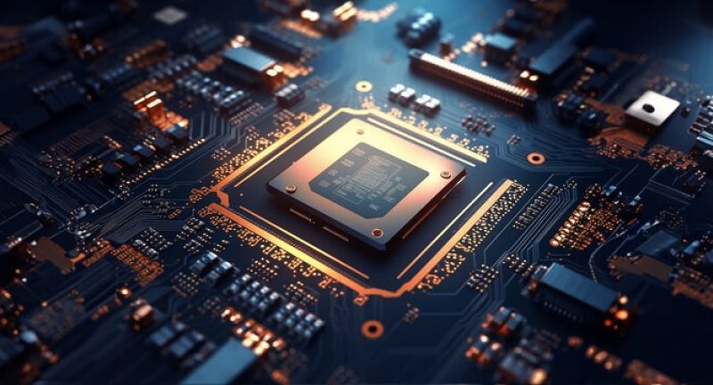
Schematic Design and Component Selection
Making circuit diagrams that show the electrical connections between components is a part of the schematic design process. Essential things to think about in this stage are:
- Component Selection: Choosing appropriate components that meet the design specifications and budget constraints.
- Schematic Capture: Using design software to create detailed schematics. This step translates the conceptual design into a precise and detailed diagram that can be used to guide the rest of the development process.
- Design Validation: Reviewing the schematics to ensure they meet all requirements. It includes checking for errors ensuring that all components are correctly connected and verifying that the design will function as intended.
Prototyping and Testing
A vital stage in the design process is prototyping, which enables PCB circuit board manufacturers to build a functional replica of the final product. This stage entails:
- PCB Design and Fabrication: Designing the printed circuit board (PCB) layout and fabricating the prototype PCB.
- Assembly: This step involves assembling the prototype with the selected components. It involves placing and soldering components onto the PCB, which creates a working prototype.
- Testing: Conducting various tests to validate the prototype’s functionality, performance, and reliability.
Firmware and Software Development
Firmware and software development are essential components of electronic devices for the design process for many electronic goods. This stage consists of:
- Firmware Development: Writing code for the microcontrollers or processors embedded in the product.
- Software Development: Building applications, control systems, and user interfaces as required.
- Integration: Ensuring seamless integration between hardware and software components.
Design Verification and Validation
Verification and validation of the design are essential to guarantee that the product satisfies all criteria in terms of standards and regulations. This phase involves:
- Verification Testing: Conducting tests to verify that the design meets all technical specifications.
- Validation Testing: Ensuring the product satisfies user expectations and performs as expected.
- Compliance Testing: Verifying that the product complies with relevant industry standards and regulations.
Pre-Production and Manufacturing
The next stage is to prepare for mass manufacturing when the design is confirmed and certified. Essential tasks in this stage consist of:
- Pilot Production: Producing a small unit batch to identify potential manufacturing issues.
- Supply Chain Management: Arranging with vendors to guarantee component availability.
- Manufacturing Planning: Coordinating with suppliers to ensure the availability of components.
Product Launch and Support
The last step in the printed circuit board layout design process is launching the product and providing ongoing support. This phase includes:
- Product Launch: Using distribution and marketing channels to bring the products to market.
- Customer Support: Offering technical support, maintenance, and updates to ensure customer satisfaction.
Feedback Collection: Obtaining user feedback to pinpoint problem areas and guide future design decisions.

Challenges One May Face
While customized electronic product design offers numerous benefits, it also presents challenges that must be navigated to ensure successful project outcomes.
Some of the common challenges include:
Complexity
Complexity in bespoke designs involves managing various components and ensuring they work harmoniously. Each custom element adds a layer of intricacy, which makes it imperative to maintain a high level of coordination among all parts.
This complexity can lead to unforeseen issues during the integration phase, requiring robust planning and problem-solving skills.
Cost
One more big obstacle is cost management. The cost of custom components is typically higher than that of off-the-shelf substitutes. Keeping these expenses within the project’s financial restrictions requires careful budgetary planning and challenging trade-offs.
Development costs can mount rapidly, especially if the desired result requires several iterations and revisions.
Time
Time constraints add further pressure. Clients typically expect timely delivery of the final product, which can be challenging given the inherent complexities of custom designs. Delays can occur due to extended development phases, unexpected technical issues, or lengthy procurement times for specialized components.
Regulatory Compliance
Regulatory compliance is a critical aspect that designers must navigate meticulously. Custom electronic products must adhere to relevant industry standards and regulations, which vary across different markets and applications. This includes meeting safety standards, electromagnetic compatibility (EMC) guidelines, and other regulatory requirements.
Incorporating compliance testing into the development process is critical, as failure to meet these standards can lead to costly redesigns, delays, and potential barriers to market entry.
That is why one must look for tips and techniques for PCB layout optimization to maximize performance.
Conclusion
Customized electronic product design meets specific business and consumer needs, drives innovation, and ensures tailored performance.
Despite its challenges—such as complexity, cost, time constraints, and regulatory compliance—success lies in meticulous planning, coordination, and adherence to standards throughout the development process.