The printed circuit board (PCB) manufacturing industry has undergone many significant improvements since the first PCB was developed in 1948. The swift advancement of technology has resulted in an ongoing demand for increasingly powerful, efficient, and compact printed electronics.
Integrating new materials is one of the primary drivers of the progress in PCB manufacturing and assembly processes. While PCBs have been used for several decades, electronics manufacturing services are leveraging new applications in various industrial sectors. This is primarily because printed electronics has made its way into almost every industry, including medical, defense, and many other vital businesses, and has impacted how they work.
Let’s look at the innovative advances in printed electronics and how new materials improve PCB efficiency and capacity.
Role of PCB in Printed Electronics
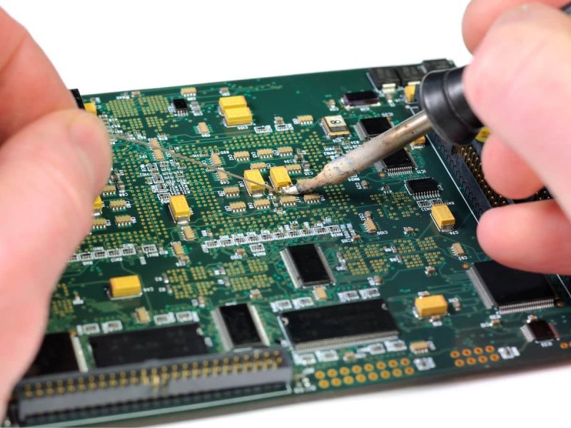
PCBs are the foundation of modern electronic devices, offering a platform for connecting and integrating diverse electrical components. PCB contract manufacturing services have traditionally been used to manufacture critical components. PCB’s narrow, flat boards include a complex network of conductive traces, components, and connectors that transmit electrical signals and power. However, the landscape has grown substantially with the introduction of printed electronics.
Printed electronics use inkjet printing, screen printing, and roll-to-roll processing to apply conductive inks and other functional materials on flexible substrates. This technique has various advantages, including cost-effectiveness, scalability, and the ability to create lightweight and compatible electronics for multiple applications.
The Need for New Materials
As the demand for smaller, lighter, and more energy-efficient electronic devices grows, there is a pressing need for innovative materials to fulfil the changing requirements of PCB fabrication and assembly. These materials must be highly conductive, flexible, thermally stable, and compatible with emerging fabrication processes.
Furthermore, the rapid growth of advanced applications such as Internet of Things (IoT) devices, wearable electronics, and intelligent systems needs the development of materials that can survive harsh environments while still performing optimally.
New Materials Redefining PCB Performance

Several new materials are redefining the field of PCB contract manufacturing, facilitating the development of unique functionality and improved performance metrics. Let’s look at some of these materials and their applications.
High-density interconnects (HDIs)
HDI materials allow for the fabrication of PCBs with smaller vias and finer line widths, resulting in increased circuit density and signal integrity. These materials are essential for addressing the requirements of high-speed digital applications and miniaturised electronic equipment. This is already widely used and in high demand as the size of digital gadgets shrinks. This technology enables small boards with limited layers to transmit signals at high speeds.
Flexible and Stretchable Materials
Flexible substrates, such as polyimide and PET, allow the fabrication of bendable and conformable PCBs, opening up new possibilities for wearable electronics, flexible displays, and biomedical implants. Similarly, stretchable materials such as elastomers and conductive inks enable the creation of PCBs that can tolerate mechanical deformation while remaining functional.
Embedded Components
Embedding passive and active components directly into the PCB substrate eliminates the need for discrete components, resulting in smaller, lighter electronic devices. This strategy improves reliability, streamlines assembly operations, and allows for the production of more compact and streamlined designs.
Integrated Circuits for IoT Devices and Smart Systems
Microcontrollers, sensors, and wireless communication modules can be integrated directly into the PCB substrate, making it easier to design IoT devices and intelligent systems with increased functionality and connection. These integrated circuits (ICs) provide seamless data sharing, real-time monitoring, and advanced decision-making in various applications, including industrial automation and smart home systems.
3D Printing and Additive Manufacturing
Additive manufacturing techniques like 3D printing provide unparalleled flexibility and customization for PCB fabrication and assembly. By precisely layering conductive and dielectric materials, 3D printing allows for the construction of complicated geometries, embedded structures, and customised interconnects that are difficult or impossible to achieve using traditional manufacturing methods.
Thermal Management Solutions
New materials with improved thermal conductivity and heat dissipation qualities are essential for tackling the thermal issues associated with high-power electronic systems. Engineers can effectively manage heat generation and maintain the reliable functioning of electronic systems under challenging conditions by including thermally conductive substrates, thermal interface materials, and heat sinks in PCB contract manufacturing.
Future Trends and Outlook
Combining printed electronics, new materials, and enhanced manufacturing processes will generate additional innovation in electronics manufacturing services. Emerging developments, such as using recyclable materials and programs, heterogeneous integration, multi-functional materials, and self-healing circuits, promise to open up new possibilities for developing intelligent, adaptive, and robust electronics.
Many chemical solutions are utilized during PCB manufacturing, and if these harmful byproducts are not correctly handled, they can contaminate the environment. Hence, many eco-friendly measures and advancements are being implemented to reduce the ecological impact. To strive toward sustainable PCB manufacturing, including using recyclable materials, such as copper and aluminum, in PCB design.
Furthermore, the continued development of environmentally friendly materials and sustainable manufacturing processes will be critical in lowering the environmental effect of electronics production and tackling global issues such as electronic waste and resource depletion.
Adopting recyclable materials to manufacture printed circuit boards (PCBs) is a forward-thinking approach. Embracing recyclable materials aligns with the global imperative to reduce electronic waste and signifies a commitment to resource conservation and circular economy principles. Polylactic acid (PLA)-based printed circuit boards (PCB) are a biodegradable alternative to traditional PCB materials. Studies also state that PLA-PCB can be easily recycled to its original components.
Some of the sustainable approaches include:
- Eco-friendly PCB materials
- Modular PCB architecture
- Green Manufacturing
- Optimized chemical usage
- PCB recycling programs
Conclusion
Printed electronics and the usage of new materials are redefining PCB fabrication and assembly, allowing for the development of next-generation electronic devices with unparalleled functionality, flexibility, and performance.
By leveraging the power of innovation and cooperation, PCB assembly manufacturers can stay ahead of the curve and promote good change in the industry.
Whether it’s creating wearable devices, powering IoT networks, or improving medical diagnostics, the opportunities for exploiting printed electronics and new materials in PCB contract manufacturing and assembly are endless.