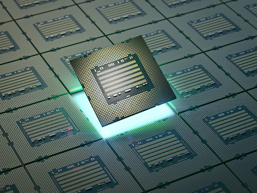
In the growing world of electronics, the printed circuit board (PCB) plays a pivotal role as the backbone of modern devices. It’s a marvel of engineering that has become an essential part of helping this industry to grow exponentially.
For PCB manufacturers, the stakes are high, and the requirements are stringent. Special processes and high reliability are not only desired but essential.
With the global PCB market size projected to reach USD 93.87 billion by 2029, growing at a CAGR of 4.28% from 2024, the industry is witnessing a surge in demand for boards that are not only functionally superior but also robust against the rigors of use.
Therefore, manufacturers are tasked with producing PCBs that can withstand extreme conditions, maintain performance over time, and support the rapid advancement of technology. Moreover, the selection of appropriate materials, precision in manufacturing processes, and adherence to quality standards are critical factors that determine a PCB’s success.
As the industry is expanding as a whole, we, as PCBLOOP manufacturers, prioritize the key industry requirements, which helps us to thrive and drive innovation in the ever-growing field of electronics.
What to know how? Come, let us show you!
Understanding High-Reliability PCBs!
Unlike a previous generation of boards that were built to withstand harsh conditions, longer life cycles, and extreme performance requirements, high-reliability boards are designed to last anywhere and solve any challenge.
Differing from commonplace consumer PCBs, which can be simply replaced if they malfunction, high-reliability boards should function perfectly for years or even decades.
Let’s explore some common scenarios where high-reliability PCBs play a critical role:
- Aerospace and Defence: Avionics systems, satellites, and military equipment demand PCBs that can withstand extreme temperatures, radiation, and mechanical stress. A single failure could have catastrophic consequences.
- Medical Devices: Implantable medical devices, diagnostic equipment, and life-saving devices rely on PCBs with exceptional reliability to ensure patient safety. Imagine a pacemaker malfunctioning due to a faulty PCB—it’s a matter of life and death.
- Automotive Electronics: From engine control units (ECUs) to safety systems, automotive PCBs must endure temperature variations, vibrations, and harsh environments. Reliability directly impacts vehicle safety and performance.
- Industrial Automation: Factory automation, robotics, and industrial control systems require PCBs that can operate continuously without failure. Downtime due to PCB issues can disrupt production lines and incur significant costs.
As these sectors rely on their technical equipment, it becomes the responsibility of a PCB assembly manufacturer to make them more reliable.
Key Requirements for High-Reliability PCB Manufacturing
To achieve high reliability, manufacturers must follow specific requirements during the PCB fabrication process:
Material Selection
- Substrates: High-temperature laminates (such as polyimide or PTFE) are preferred for their thermal stability. These materials can withstand elevated temperatures without compromising structural integrity.
- Copper Foil: Thick copper layers enhance current-carrying capacity and reduce impedance. Adequate copper thickness ensures efficient power distribution and minimizes voltage drops.
Design Considerations
- Trace Width and Spacing: Wider traces reduce resistance and improve reliability. Properly designed trace widths prevent overheating and signal degradation.
- Via Placement: Properly positioned vias prevent signal integrity issues. Blind vias and buried vias allow for complex multilayer designs without compromising reliability.
Special Processes for High-Reliability PCB Manufacturing
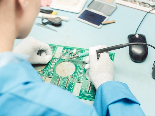
Let us show manufacturers the special processes to create high-reliability PCBs.
High-Density Microvia (HDI) Fabrication
HDI technology enables the best PCB fabrication with a higher density of vias and interconnections. This is achieved through the use of microvias, which are small holes with diameters typically less than 150 micrometres.
These microvias can be drilled using laser or mechanical methods and connect different layers of a PCB in a much smaller area than traditional vias.
The HDI process allows for finer lines and spaces, higher connection pad density, and improved electrical performance, making it ideal for compact, high-performance devices.
Blind and Buried Vias
Blind vias connect an outer layer to one or more inner layers but do not go through the entire board. On the other hand, Buried vias are located within the board and connect two or more internal layers without reaching the outer layers.
These vias are essential for multi-layer PCBs where space is at a premium. They help to maintain signal integrity by reducing the path length of signals and minimizing electromagnetic interference.
Controlled Impedance Routing
Controlled impedance routing is critical in maintaining signal integrity, especially in high-speed applications. It involves configuring the dimensions of the PCB traces to match a specified characteristic impedance.
The process ensures that the signal travelling through the traces retains its integrity, minimizing signal loss and reflections. This process requires precise calculation and design to match the impedance of the traces with the components and connectors.
Advanced Soldermask and Legend Finishes
The solder mask is a protective layer applied to the PCB to prevent solder bridging and protect copper traces from oxidation and environmental damage. Advanced soldermask technologies provide better resolution, allowing for finer pitch components.
The legend, or silkscreen, provides important information on the PCB, such as component identifiers and test points. Advanced finishes can improve the durability and readability of these markings.
Selective Plating
Selective plating involves applying metal coatings, such as gold or nickel, to specific areas of the PCB, typically the contact pads or connectors. This enhances conductivity, corrosion resistance, and solderability. Gold plating is often used for edge connectors due to its excellent conductivity and resistance to wear.
Conformal Coating
Conformal coating is a thin polymeric film applied to a PCB to protect it from moisture, dust, and chemical exposure. It conforms closely to the board’s topography, providing insulation and sealing out contaminants.
Conformal coatings are typically applied at thicknesses of 25-75μm and are essential for ensuring the longevity and reliability of the PCB in harsh environments.
These processes collectively contribute to the production of high-reliability PCBs that can withstand demanding conditions and meet the rigorous standards required for critical applications.
Why are Special Processes Crucial for High Reliability?
- These processes enhance durability, thermal performance, and signal integrity.
- They minimize the risk of defects, such as shorts, opens, and delamination.
- High-reliability PCBs undergo rigorous testing to ensure compliance with industry standards (e.g., IPC-A-600, MIL-PRF-31032).
Considerations and Challenges for PCB Manufacturers
- Cost: Implementing special processes increases manufacturing costs. However, the long-term benefits outweigh the initial investment.
- Complexity: Designing and fabricating HDI boards, managing impedance, and applying conformal coatings require expertise.
- Supply Chain: Sourcing reliable materials and components is essential for consistent quality.
PCBLOOP as a Solution
The demand for dependable PCBs in critical applications is surging. At PCBLOOP, we’re more than a PCB assembly manufacturer – we’re your partner in high-performance, reliable PCBs.
Our expertise in special processes – HDI, advanced vias, controlled impedance – ensures top-notch functionality and durability. We go beyond technology with meticulous material selection, expert design considerations, and unmatched quality standards. Moreover, we offer cost-effective solutions, in-house expertise, and a reliable supply chain.
So, don’t compromise on reliability. Let PCBLOOP be your partner in creating the best PCB fabrication that pushes the boundaries of functionality and endurance.
Contact us today to discuss your specific requirements and experience the PCBLOOP difference.