
Did you know the global printed circuit board (PCB) market is projected to surpass $83.48 billion by 2028 at a CAGR of 5.7%, driven by the increasing demand for compact, high-performance electronic devices?
As modern technology advances at an unprecedented pace, the importance of efficient PCB layout design cannot be overstated.
A well-designed PCB layout forms the backbone of reliable electronic products, ensuring optimal performance, signal integrity, and minimal manufacturing errors.
In fact, according to a study by Transparency Market Research, flexible PCBs alone are expected to reach 37.9 billion U.S. dollars by 2031 and will grow at a CAGR of 12.5% between 2023 and 2031 due to their increasing use in medical devices, automotive electronics, and consumer products. This reflects the growing significance of advanced PCB layouts in high-tech applications.
In this blog, we’ll explore essential PCB layout techniques and breakthroughs that help create flawless electronic products while highlighting the role of professional PCB layout services in the design process.
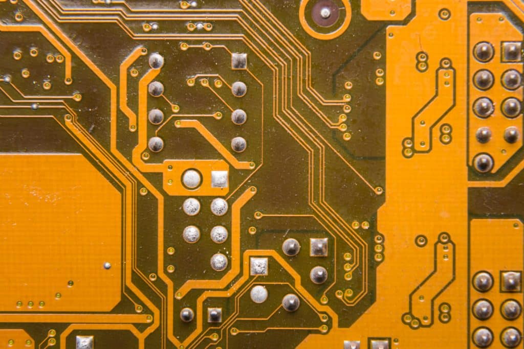
Importance of a Well-Designed PCB Layout
A well-designed PCB layout is crucial to ensuring electronic products’ efficiency, performance, and reliability. Manufacturers can create high-quality devices that meet today’s technological demands by focusing on signal integrity, minimizing errors, and optimizing the overall design.
- Ensuring Signal Integrity and Performance
One of the primary objectives of a well-designed PCB layout is to ensure signal integrity and maintain overall performance. Signals passing through traces on a PCB are prone to interference, crosstalk, and electromagnetic interference (EMI) if the layout isn’t optimized. Signal integrity ensures electrical signals maintain their quality and strength throughout the PCB, preventing data loss or degradation.
By employing an expert PCB layout service, you can ensure that your design implements proper trace routing, shielding, and grounding, which are crucial to preserving signal strength and reducing noise. A well-designed layout minimizes performance issues, resulting in a product that functions reliably over time.
- Minimizing Manufacturing Errors
A poorly designed PCB layout can lead to costly manufacturing errors such as short circuits, component misalignments, or incomplete solder joints. Issues like incorrect spacing between traces or improperly placed vias can lead to defective products requiring rework or scrapping.
A professional PCB layout service can help mitigate these risks by adhering to design rules and best practices during the layout process. This ensures that the final product is defect-free, reducing production costs and improving time to market.
Essential PCB Layout Techniques for High-Quality Electronic Products
Implementing key PCB layout techniques effectively is crucial to achieving the highest quality in electronic products. One foundational technique is component placement optimization, which plays a vital role in enhancing the overall design and performance of the PCB.
- Component Placement Optimization
Optimized component placement is critical to achieving a functional and efficient PCB design.
Maximizing performance through PCB layout optimization ensures that strategically placing components improves power distribution, heat management, and signal flow. For example, high-power components should be placed near power sources, while sensitive components should be isolated to reduce interference.
By leveraging the expertise of a PCB layout service, designers can ensure that component placement is optimized to balance performance, power efficiency, and manufacturability, resulting in a robust final product.
- Trace Routing & Via Strategies
Trace routing involves designing the copper pathways that carry signals between components on the PCB. Proper trace routing techniques, such as minimizing trace lengths and avoiding sharp angles, help maintain signal integrity and reduce noise. Additionally, differential pairs should be used for high-speed signals to prevent further interference.
Via strategies, on the other hand, focus on using vias (small copper-plated holes) to connect different layers of the PCB. Proper use of vias ensures that signals are transferred between layers efficiently. High-performance designs often incorporate blind or buried vias to minimize space usage and maintain signal quality.
An expert PCB layout service can guide you in choosing the right trace routing and via strategies to maximize performance without increasing complexity.
- Ground and Power Plane Consideration
Ground and power planes are essential for stabilizing voltage levels and reducing electromagnetic interference (EMI). A continuous ground plane provides a low-impedance path for return currents, while a well-designed power plane ensures even power distribution across the board.
These planes also help reduce signal noise and improve overall circuit stability, especially in high-frequency designs. Choosing the right PCB manufacturer for PCB layout service ensures proper power and ground plane configuration, leading to a reliable, high-performance product.
- Signal Layer Stackup
Multi-layer PCBs often use signal layer stacking to efficiently organize and manage signal flow. In a well-structured stacking, signal layers are arranged between ground and power planes to minimize noise and cross-talk. Proper stacking design also helps with impedance control, a critical factor in maintaining signal integrity in high-speed circuits.
When working with a professional PCB layout service, designers can optimize the signal layer stack to achieve the best balance between performance and cost while reducing potential issues during manufacturing.
Key Breakthroughs in PCB Layout Design
- High-Density Interconnect (HDI) Technology
High-Density Interconnect (HDI) technology is a game-changer in PCB design, enabling manufacturers to pack more functionality into smaller spaces. HDI PCBs feature finer lines, smaller vias, and more densely packed components, making them ideal for compact devices like smartphones and wearables.
HDI technology also improves signal integrity and allows for faster data transmission, making it an essential element in high-performance applications. Partnering with a PCB layout services experienced in HDI technology can help create compact, high-speed products with exceptional performance.
- Flex and Rigid-Flex PCBs
Flex and rigid-flex PCBs are another key breakthrough in modern PCB design. Flex PCBs use flexible materials that can bend and fold, allowing for versatile, lighter, and more durable product designs. Rigid-flex PCBs combine flexible and rigid layers, offering greater design flexibility while maintaining structural integrity.
These advanced PCB types are increasingly used in aerospace, medical devices, and automotive electronics industries, where space-saving designs are crucial. A PCB layout service specializing in flex and rigid-flex designs can ensure the proper integration of these innovative technologies.
- Embedded Components and 3D PCB Design
Embedded components and 3D PCB design have revolutionized the way PCBs are structured. By embedding components directly into the PCB layers, designers can reduce the board size while improving performance. 3D PCB designs, which involve stacking layers or mounting components on multiple sides, offer further space-saving advantages and design flexibility.
This breakthrough technology is especially useful for complex, high-performance devices where space is at a premium. Working with a PCB layout service that understands embedded components and 3D design can help manufacturers stay ahead in a competitive market.
Conclusion
A well-designed PCB layout is the foundation for creating high-performance, reliable electronic products. By optimizing component placement, trace routing, via strategies, and power and ground plane considerations, manufacturers can minimize signal degradation and manufacturing errors. Furthermore, breakthroughs in PCB technology, such as HDI, flex and rigid-flex PCBs, and 3D designs, have opened new possibilities for creating compact, high-quality devices.
Partnering with PCBLOOP ensures that all of these critical factors are addressed, resulting in efficient, high-quality electronic products that meet today’s market demands. As technology evolves, PCB layout techniques and innovations will remain key to producing the next generation of cutting-edge devices.