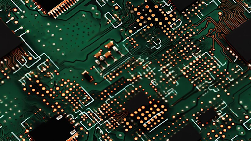
Printed Circuit Boards, or PCBs, are at the heart of modern electronic devices, from smartphones to advanced medical equipment. Before a PCB design moves to physical production, it’s essential to ensure that the board will perform as expected.
This is where PCB simulation and validation methods come into play. Validating electronic ideas through PCB simulation ensures that electronic assembly works seamlessly, saving time, money, and resources by minimizing errors early in the design process.
Due to technological advancements in developing PCB design tools and integrating 3D design and visualization technologies, North America held a 37% global market share in the PCB design software market in 2021. This demonstrates the growing importance of simulation and validation in meeting market demands.
Here, you will explore various PCB simulation and validation methods, the importance of testing before assembly, and how companies like PCBLOOP can help streamline the process.
Importance of PCB Validation and Simulation
The benefits of PCB simulation and validation are numerous. By simulating the electrical characteristics, thermal performance, and mechanical integrity of a PCB, designers can:
- Identify and Rectify Design Flaws
Before they become expensive errors, simulation assists in identifying possible problems such as open circuits, short circuits, signal integrity difficulties, and excessive heat generation.
- Optimize Component Placement
By analyzing the effects of component placement on factors like signal integrity and electromagnetic interference (EMI), designers can optimize the layout for optimal performance.
- Validate Design Rules
Simulation ensures compliance with design rules and standards, preventing manufacturing defects and ensuring reliable operation.
- Reduce Time-to-market
Simulation can significantly reduce the development cycle and accelerate product launch by identifying and addressing issues early in the design process.
- Enhance Product Reliability
Thorough validation helps to identify and mitigate potential failure modes, leading to more reliable and durable products. Important simulations and testing for PCB reliability also ensure long-term durability and functionality.
PCB Simulation Method
Various PCB simulation tools and techniques are available to address different design requirements. Some of the most commonly used methods include:
- Circuit Simulation
Circuit simulation helps evaluate how a PCB will function in the real world by modeling electronic components and their interactions. It simulates a circuit’s voltage, current, and power, allowing designers to catch problems early on.
Tools such as the Simulation Program with Integrated Circuit Emphasis (SPICE) are commonly used for circuit-level simulations. Designers can modify parameters, such as resistances and voltages, to assess their impact on the PCB’s performance.
- Signal Integrity Analysis
Signal integrity simulation is essential when dealing with high-speed circuits. This method ensures that the signals transmitted through the PCB are not distorted by noise or delays. Signal integrity problems can cause data corruption, especially in digital circuits.
Using SI simulation, designers can evaluate how the signal will travel across traces and interconnects in the PCB. Signal integrity issues cause most PCB failures in high-speed circuits.
This makes SI simulation a critical aspect of the PCB validation process, particularly in the era of faster communication devices.
- Power Integrity Analysis
Power integrity simulation assesses the power distribution network (PDN) of a PCB to ensure the proper delivery of power to all components. Inadequate power delivery can lead to voltage drops or surges, impacting the performance of sensitive components. PI simulation helps designers optimize the power layout and avoid potential failures.
- Thermal Analysis
This assesses the temperature distribution on the PCB to prevent overheating and component failure. Tools like Ansys Icepak and Flotherm are used for thermal simulation.
- Electromagnetic Interference (EMI) Analysis
Electromagnetic interference can disrupt the operation of other nearby devices and lead to non-compliance with regulatory standards. EMI simulation ensures that the PCB design does not generate interference that exceeds acceptable levels.
This method is particularly important for products like wireless communication devices or medical electronics. Using EMI simulation, designers can detect potential interference issues early, preventing costly rework.
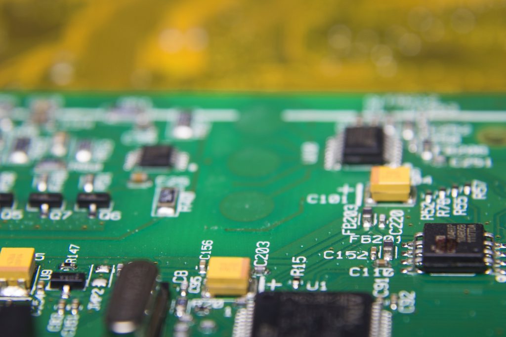
Physical Validation Methods
In addition to simulation, physical validation techniques help confirm that a PCB performs as expected once manufactured.
- Design for Manufacturability Check
DFM is the process of validating a PCB design to make sure it can be efficiently manufactured without defects. DFM checks assess factors such as trace width, spacing, and component placement.
- Design Rule Check (DRC)
Design rule checks are automated processes that compare a PCB design against specific rules or guidelines. DRC identifies problems related to trace width, spacing, pad sizes, and clearances. Ensuring compliance with these rules minimizes the chances of manufacturing errors.
- Prototype Testing
Although simulation covers many potential issues, creating a physical prototype allows engineers to test the design under real-world conditions.
Prototype testing is particularly important when dealing with complex designs where simulations may not capture every possible failure mode. Physical testing includes functional testing, environmental testing, and reliability testing.
Tools for PCB Simulation and Validation
Various recommended efficient PCB design software or tools are available for PCB simulation and validation. Some popular ones include:
- Altium Designer: Known for its integrated PCB design environment, it offers robust tools for circuit simulation, SI, and EMI analysis.
- Cadence Allegro: This tool provides advanced PCB design capabilities with powerful signal and power integrity simulation options.
- Ansys HFSS: A specialized tool for electromagnetic simulation that analyzes high-frequency PCBs and ensures EMI compliance.
How PCBLOOP Supports Electronic Assembly Validation?
The U.S. and Europe PCB design market is predicted to reach USD 3 billion by 2035, growing at a CAGR of 5% from 2023.
Therefore, by integrating advanced simulation tools with practical validation methods, PCBLOOP helps designers avoid costly mistakes and streamline manufacturing processes in the PCB design market.
PCBLOOP, a trusted name in electronic assembly, offers a comprehensive suite of services to validate PCB designs before they move into production.
Key Services Offered by PCBLOOP
- Comprehensive Simulation Tools: These tools provide access to cutting-edge simulation technologies, including SI, PI, and EMI simulation, to ensure flawless design validation.
- Prototype Testing: PCBLOOP has in-house facilities for prototype creation, which allows engineers to test their designs and physically validate them under real-world conditions.
- DFM Analysis: PCBLOOP’s experts run DFM checks to ensure the PCB design is optimized for efficient manufacturing without risking defects.
Conclusion
Validating electronic ideas through PCB simulation and validation methods is crucial to ensuring the success of any electronic assembly project. Using simulation tools like circuit analysis, signal integrity, and electromagnetic interference validation can significantly reduce the risk of design errors. Physical validation methods like DFM checks and prototype testing complement simulation efforts by ensuring that PCBs are manufactured and functional in real-world conditions.
As electronics evolve in complexity, the need for efficient PCB validation methods has never been more important.
Companies like PCBLOOP play a pivotal role in ensuring the reliability and success of electronic assemblies by offering comprehensive simulation and validation solutions. By partnering with PCBLOOP, designers can confidently move their ideas from concept to reality, knowing that their designs are thoroughly validated and optimized for production.
By leveraging these tools and methodologies, you can ensure a successful electronic assembly process, reduce time to market, and avoid costly mistakes.